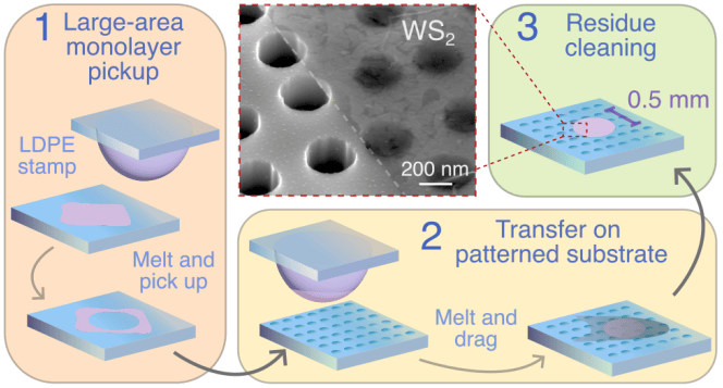
Check out our recent publication in ACS Nano, where we present a new approach for transferring 2D materials onto patterned surfaces over large areas. Using deterministic stamping, we demonstrate the integration of atomically thin materials with nanoscale topography while maintaining high-quality interfaces. This approach enables scalable fabrication of hybrid 2D-material structures and provides new opportunities for integrating 2D materials with photonic and electronic devices.
 Van de Groep Lab